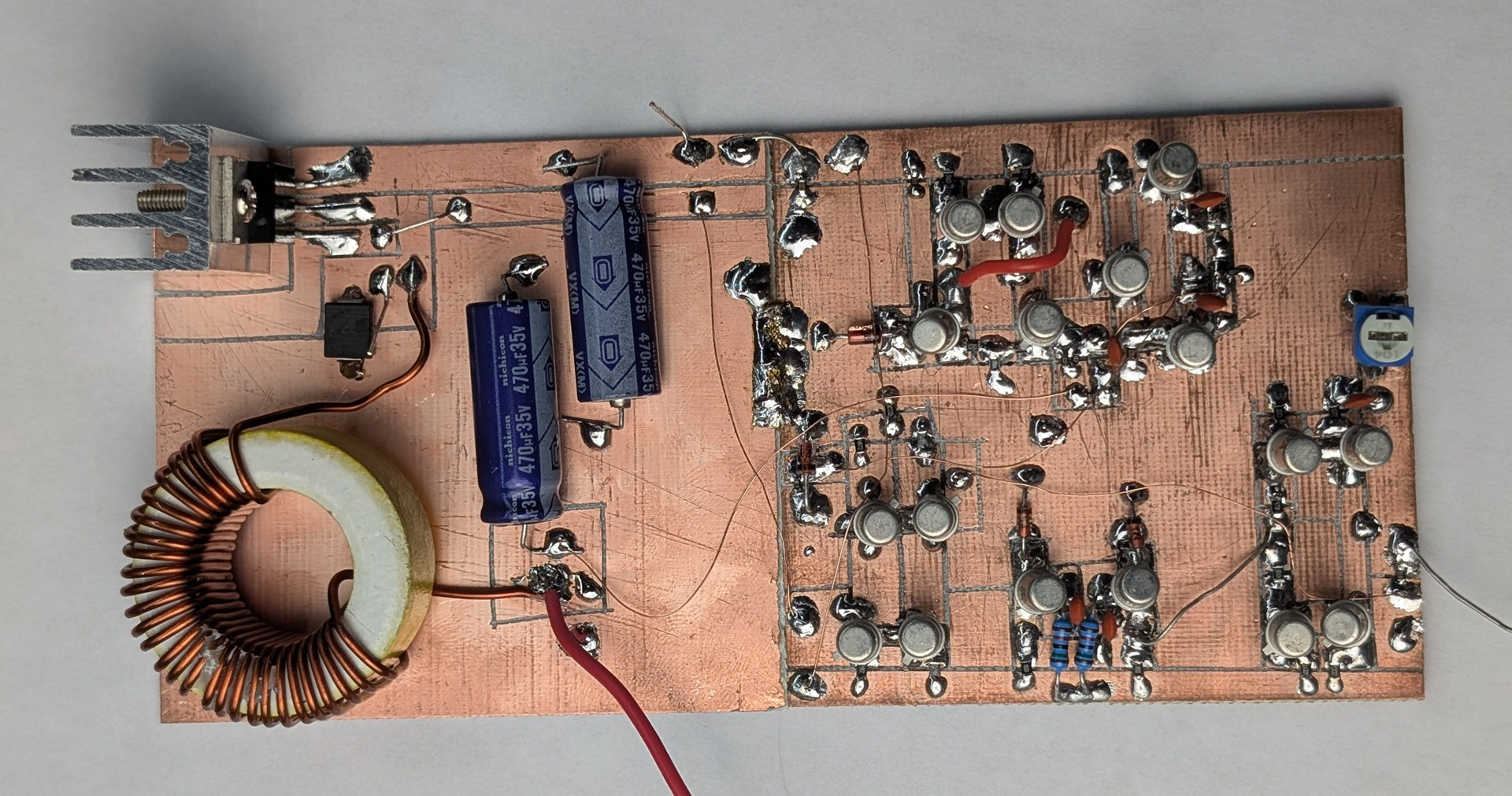
Fully discrete buck converter
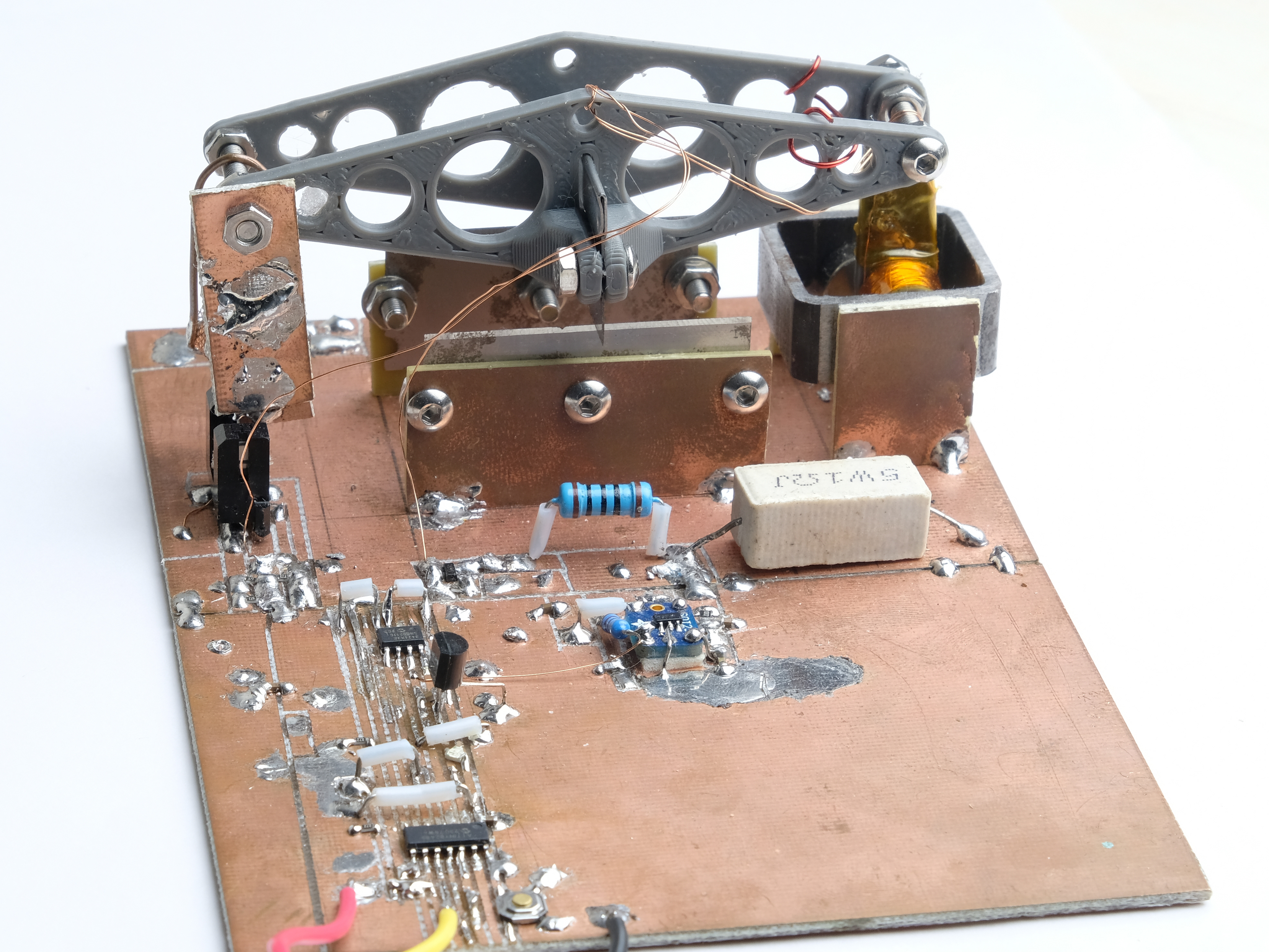
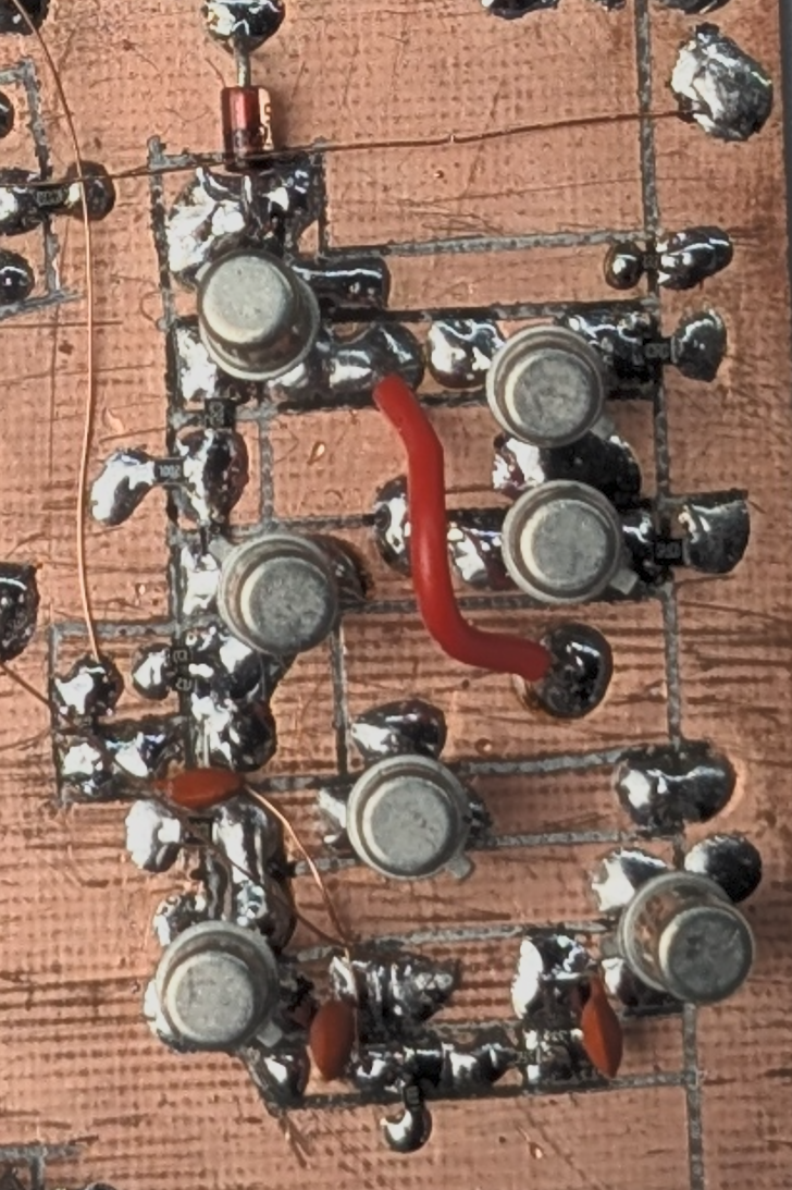
The above image shows a 9V to 5.4V buck converter using only discrete components. I made it as a final project for my power management circuits class. It uses 17 BJTs, a PFET, and several diodes.
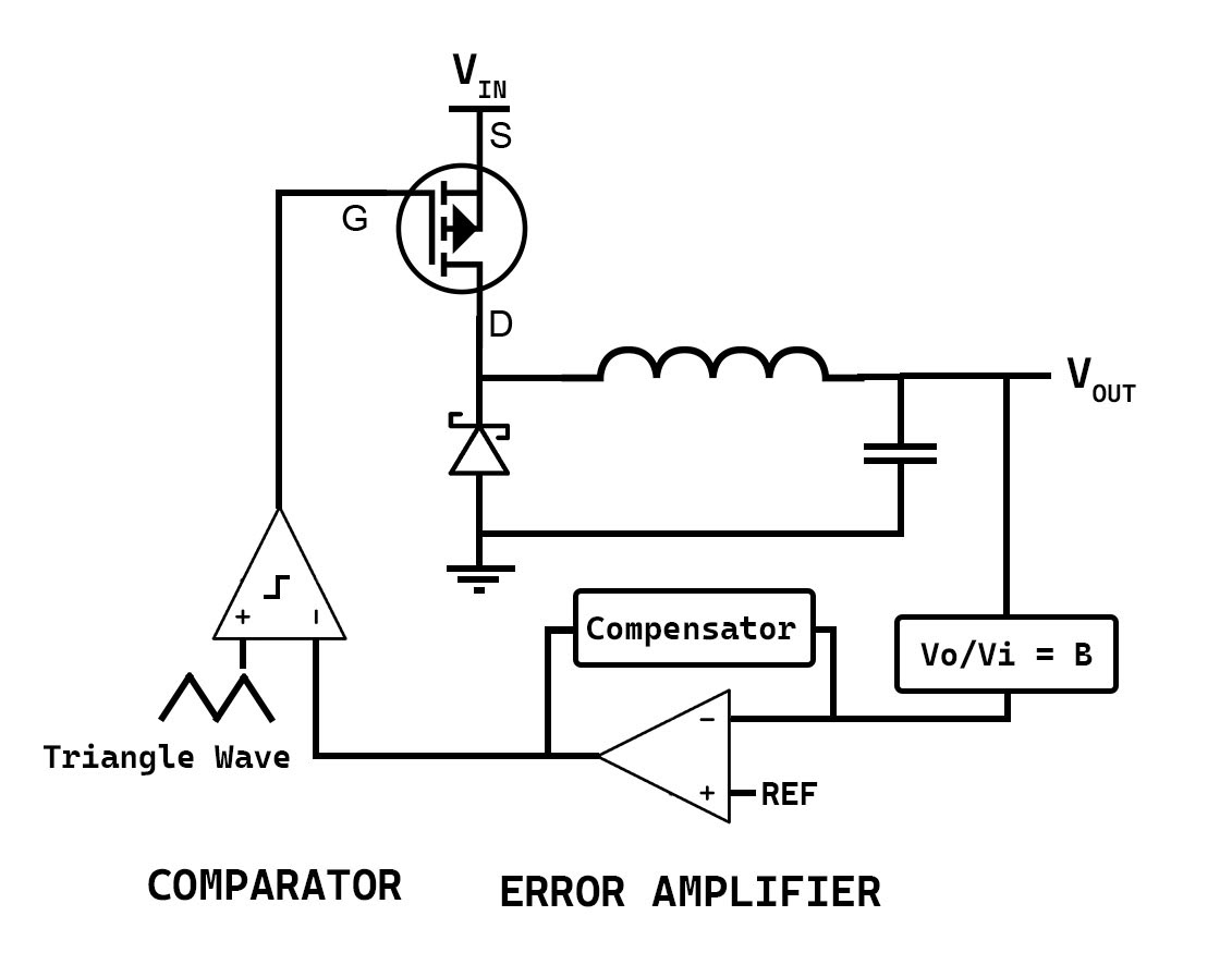
The diagram above shows the basic architecture of a buck converter. A high side switch is driven by PWM control at some duty cycle D, producing an output with an average voltage of D*Vin. The inductor and capacitor form an LC low pass filter to turn this into a constant DC output voltage. A low-side switch, either another FET or a diode, provides a current path for the inductor current when the other switch is open.
The filtered output voltage is sampled via a divider with ratio B. The difference between B*Vout and the reference voltage is amplified into an error voltage and sent to a comparator. On the other input of the comparator is a triangle wave. This setup produces a square wave out of the comparator with a duty cycle proportional to the error voltage.
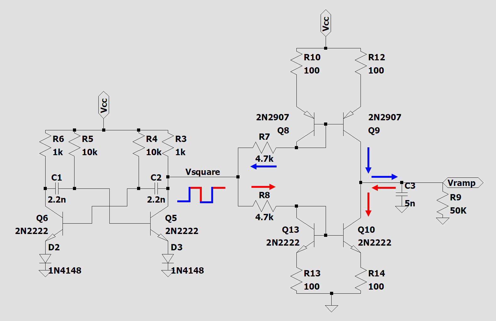
The triangle wave generator starts with an astable multivibrator which produces a square wave at a frequency of about 30 kHz. When its output is low, a constant current is pulled out of R7. By the action of the high-side current mirror, an equal current is pushed into C3. Likewise, when the square wave is high a current is pushed into R8 and thus pulled out of C3. The constant currents charging and discharging this capacitor form a linear voltage ramp. R9 is provided to compensate for any lingering current in the right side of the mirrors which would have a tendency to drive the capacitor voltage towards the rails.
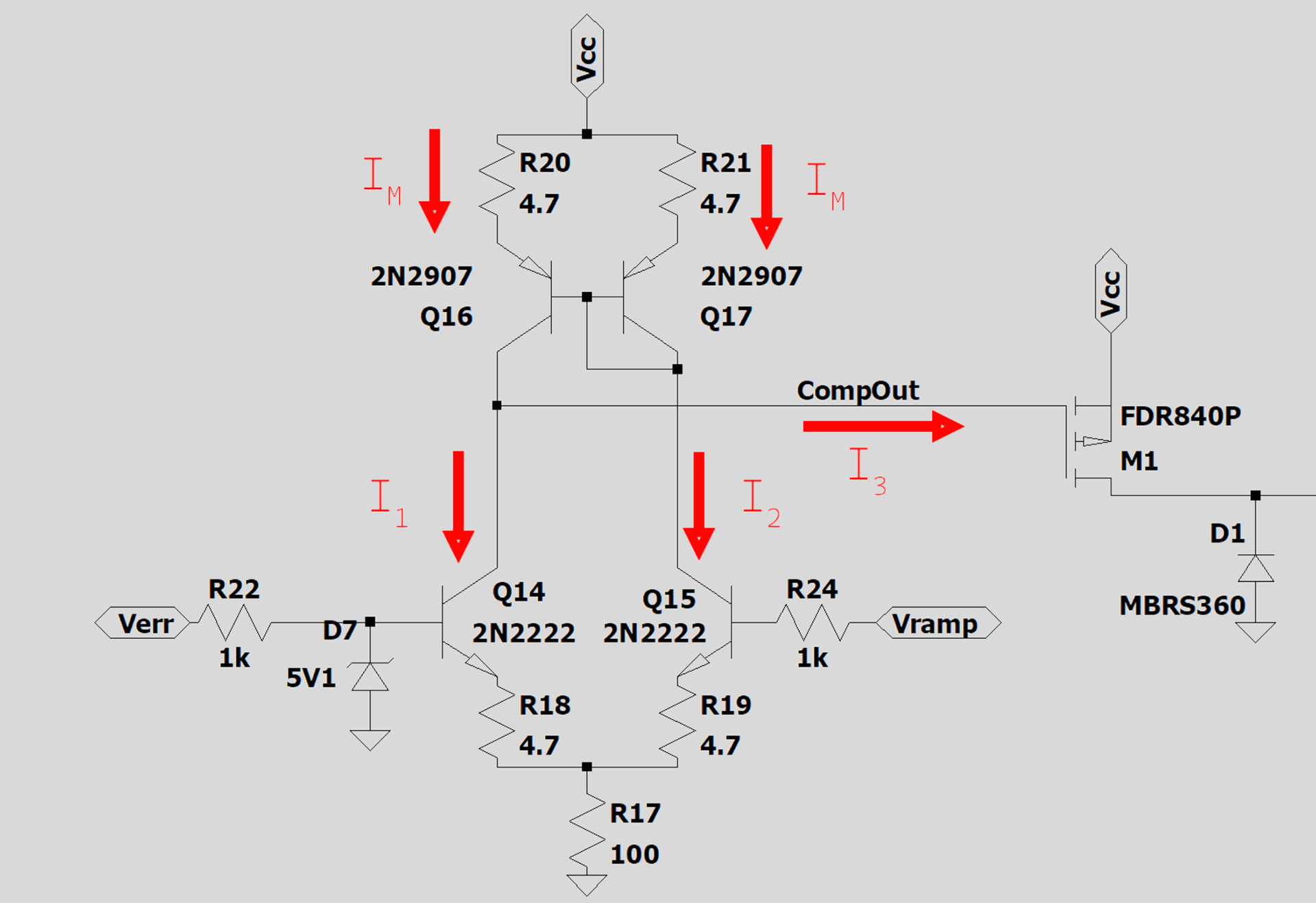
The comparator produces a PWM drive for the switching transistor by comparing the error voltage with a triangle wave. It is based around a differential pair and a current mirror. The mirror current, set by Vramp, is pushed into both transistors of the differential pair. If Verr is less than Vramp then I1 will be less than I2, so the excess current is forced into I3, turning off the FET. In the opposite case current is pulled from I3 and the transistor turns on. This relationship between currents holds until the gate is either fully charged or discharged and the current must stop. Then the mirror transistors enter saturation and the analysis no longer applies.
The PFET is turned on when the PWM signal is low, so the duty cycle is measured by the proportion of the time CompOut is low. This duty cycle increases as the error voltage increases. Because the error amplifier is inverting, an increase in error voltage implies a drop in the output voltage. This is the fundamental operation of a buck converter: when more current is drawn from the output and its voltage drops, the duty cycle increases to deliver more current from the supply to the output and return the voltage to its intended value.
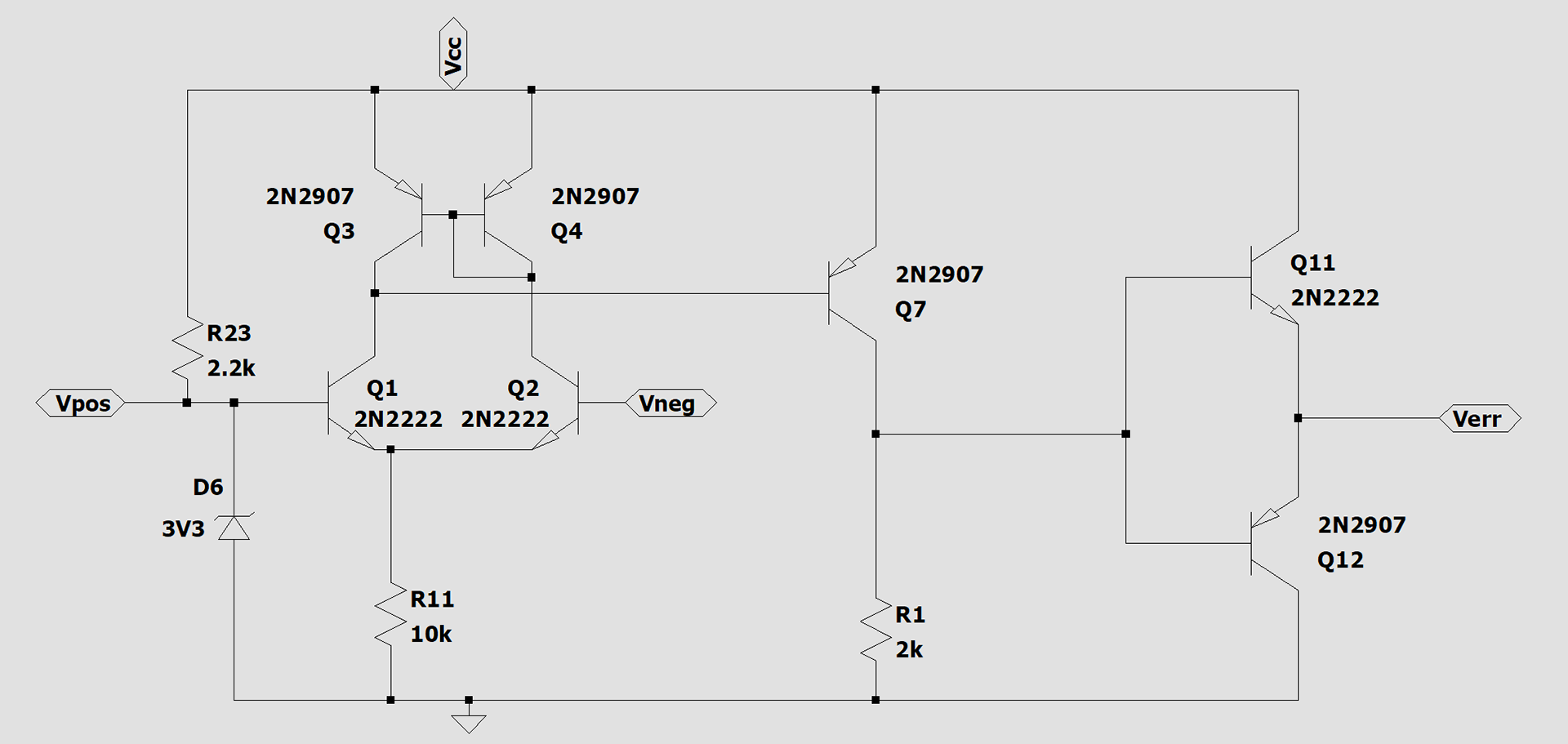
The error amp is a textbook 3 stage op amp. At the input is a differential pair, biased by R11 and with a current mirror on the collectors. An output current proportional to Vpos-Vneg is sent to the base of Q7, which forms the voltage amplifier stage. Its output is buffered by Q11 and Q12. The amplifier has about 60dB of open loop gain and its first internal pole is at about 100kHz. There is no Miller compensation so the amplifier isn't unity gain stable, but this doesn't matter it is only operated with the attached compensation network. It is important that the amplifiers internal pole is beyond the converters overall unity gain frequency (which in this case is about 5 kHz) so that its phase contribution doesn't lead to instability.
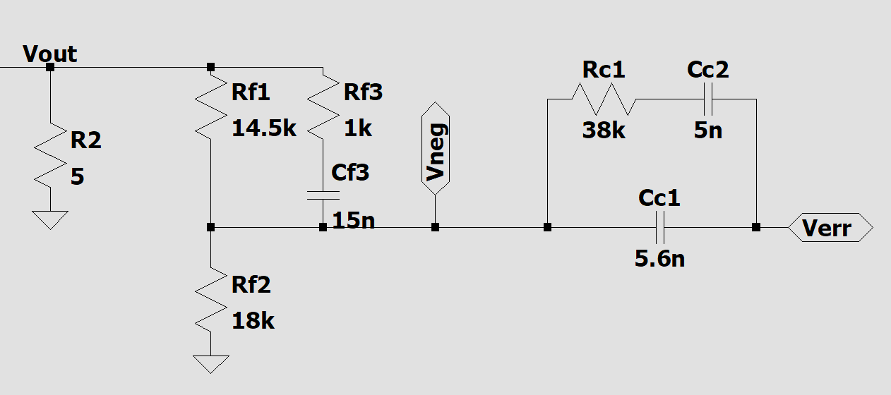
A compensation network is required on the error amplifier. As with any buck converter, the two resonant LC poles, in combination with other parasitic poles or RHP zeroes, produce enough phase shift that the system is unstable. The compensator is of Type 3 architecture. It introduces a DC pole and two zeroes just before the LC poles (it also introduces two more high frequency poles, but they are beyond the unity gain frequency of the system). This stabilizes the loop. For more information on buck converter compensation, I suggest this application note by TI.
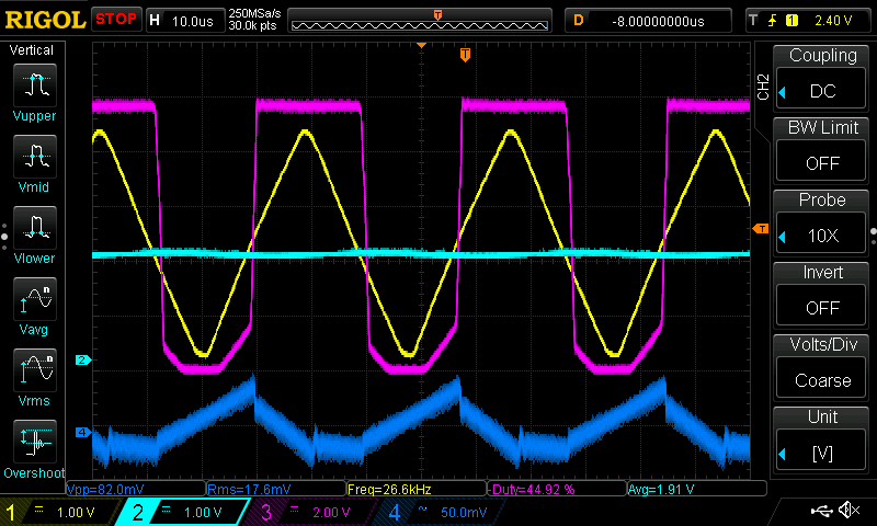
The image above shows several waveforms of the converter's operation. In yellow is Vramp, the output of the triangle wave generator. In light blue is Verr, the output of the error amplifier. Purple shows the output of the comparator which drives the PFET. Dark blue shows the AC ripple on the output voltage.
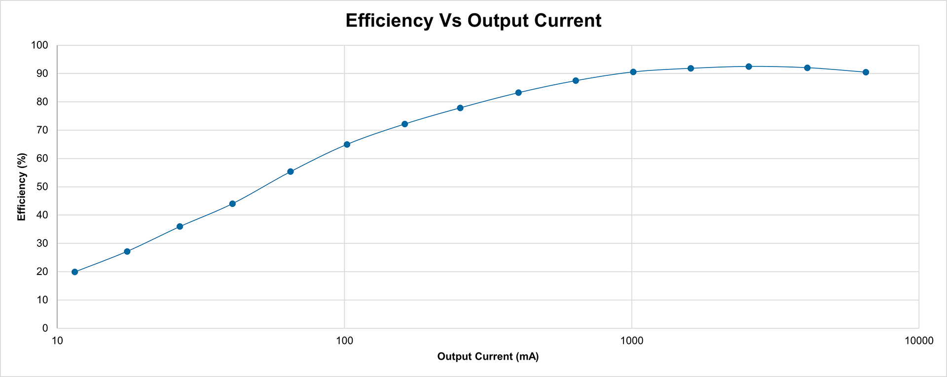
The converter has very poor efficiency at low loads, due both to the ~30mA quiescent current draw of the control circuitry and the fact that the comparator bias current, and thus PFET drive current, is reduced when Verr is low. At high loads it achieves a respectable conversion efficiency, peaking at about 92% with an output current of 2.5 amps.